...the who's who,
and the what's what 
of the space industry

Space Careers

news Space News

Search News Archive

Title

Article text

Keyword

  • Home
  • News
  • ESA's new dimension in printed circuit design

ESA's new dimension in printed circuit design

Written by  Monday, 30 October 2023 12:03
Write a comment
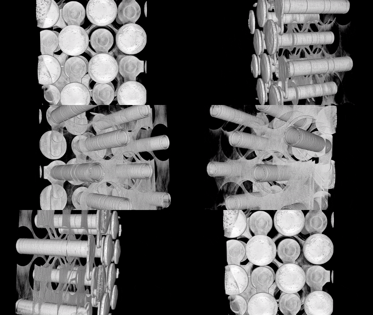
X-ray tomographic view of Printed Circuit Board microvias

This microscopic X-ray animation shows one of the key technologies allowing advanced computer functionality to fit within the smartphone in your pocket: ‘microvias’ are laser drilled holes a small fraction of a millimetre in diameter. A typical high-density interconnect printed circuit board might possess thousands of microvias, which serve to connect multiple functional layers.

ESA's HDI PCB technology roadmap

Specific HDI PCB qualification was, so far, not available as per the generic PCB guidelines of the European Cooperation for Space Standardization, ECSS – the common European rulebook for undertaking space missions. Instead, case-by-case project qualification is required for individual designs and batches, which is a significant hurdle in space projects.

But now PCB manufacturer ACB in Dendermonde, Belgium, has received ESA qualification for HDI PCBs, as the successful outcome of a recent General Support Technology Programme contract led for ESA by Belgian research institute IMEC, with Thales Alenia Space Belgium as end user.


Read more from original source...

You must login to post a comment.
Loading comment... The comment will be refreshed after 00:00.

Be the first to comment.

Interested in Space?

Hit the buttons below to follow us...